As an electronic person, the basic knowledge of digital circuits is something that everyone must master, and the same is true for electronic people who learn PCB design. Today, 2PCB mainly introduces the combinational logic circuits in digital circuits.
About combinational logic circuits
The circuit that uses digital signals to perform arithmetic and logical operations on digital quantities is called a digital circuit, or a digital system. Because it has logical operations and logical processing functions, it is also called a digital logic circuit.
According to the different characteristics of logical functions, digital circuits can be divided into two categories, one is called combinational logic circuits (combinatorial circuits for short), and the other is called sequential logic circuits (sequential circuits for short). The characteristic of the combinational logic circuit in terms of logical function is that the output at any time depends only on the input at that time, and has nothing to do with the original state of the circuit.
The logical function of the combinational logic circuit is as follows:
Li=f(A1, A2, A3…An) (i=1, 2, 3…m)
Among them, A1~An are input variables, and Li is the output variable.
Combinational logic circuit analysis
Analysis steps:
(1) Write the output logic function expression according to the logic circuit diagram;
(2) List the truth table according to the logic expression;
(3) Analyze the circuit function from the truth table or expression.
Commonly used combinational logic circuits
Commonly used combinational logic circuits include: arithmetic operation circuits, encoders, decoders, data selectors, data distributors, numerical comparators, etc.
1. Arithmetic operation circuits
a. Half adder and full adder
When two numbers A and B are added, only the sum of the base position is calculated, and the carry number sent from the lower position is not considered. This is called “half addition”. The logic circuit that completes the half addition function is called a half adder. When two numbers are added, not only the sum of the base position but also the carry number from the lower position is considered. This is called “full addition”. The logic circuit that realizes this function is called a full adder.
b. Adder
The circuit that realizes the addition of multi-bit binary numbers is called an adder. According to the different carry modes, there are two types: serial carry adder and carry lookahead adder.
2. Encoder
The process of using code to represent a specific signal is called encoding; the logic circuit that implements the encoding function is called an encoder. The input of the encoder is the encoded signal, and the output is a set of binary codes corresponding to the input signal. Encoders include ordinary encoders and priority encoders.
3. Decoder
The process of converting binary codes into corresponding output signals is called decoding. The logic circuit that completes the decoding function is called a decoder. The n inputs and m outputs of the decoder should satisfy 2n≥m. Decoders include binary decoders, binary-decimal decoders, digital display decoders, etc.
4. Data selector
Data selector is a combinational logic circuit that selects a specified one from a group of input signals and sends it to the output end according to the given input address code. Sometimes it is also called a multiplexer or multiplexer.
5. Data distributor
The circuit that can transmit 1 input data to any of the m output ends as needed is called a data distributor, also known as a multiplexer, and its logical function is exactly the opposite of the data selector.
6. Numerical comparator
In digital circuits, it is often necessary to compare two binary numbers with the same digits to determine their relative size or whether they are equal. The logic circuit used to implement this function is called a numerical comparator.
Combinational logic circuit design
General steps:
(1) List the truth table based on the actual logic problem;
(2) Write the logic expression based on the truth table;
(3) Simplify and transform the output logic expression;
(4) Draw a logic diagram.
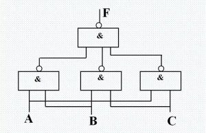
Example: Try to use NAND gates to design a three-variable voting circuit, and the voting rule is that the minority obeys the majority.
Solution: (1) List the truth table
Assume: A, B, and C represent the three input variables, and F represents the voting result. And let A, B, and C be 1 for approval and 0 for opposition; F is 1 for approval and 0 for rejection.
(2) Simplify and find the simplest function expression

(3) Draw the circuit diagram